Description:
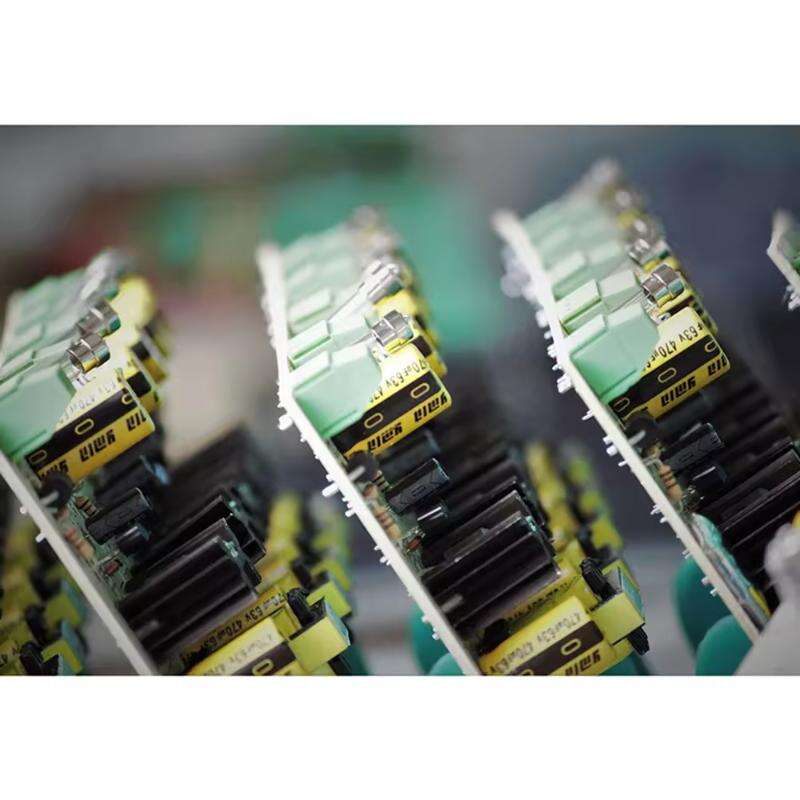
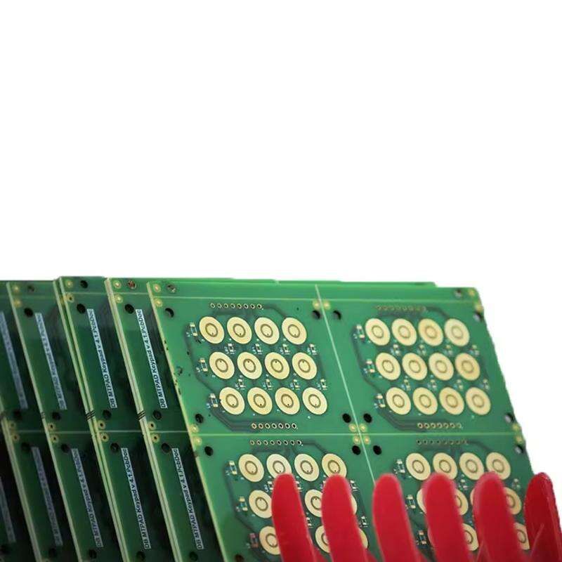
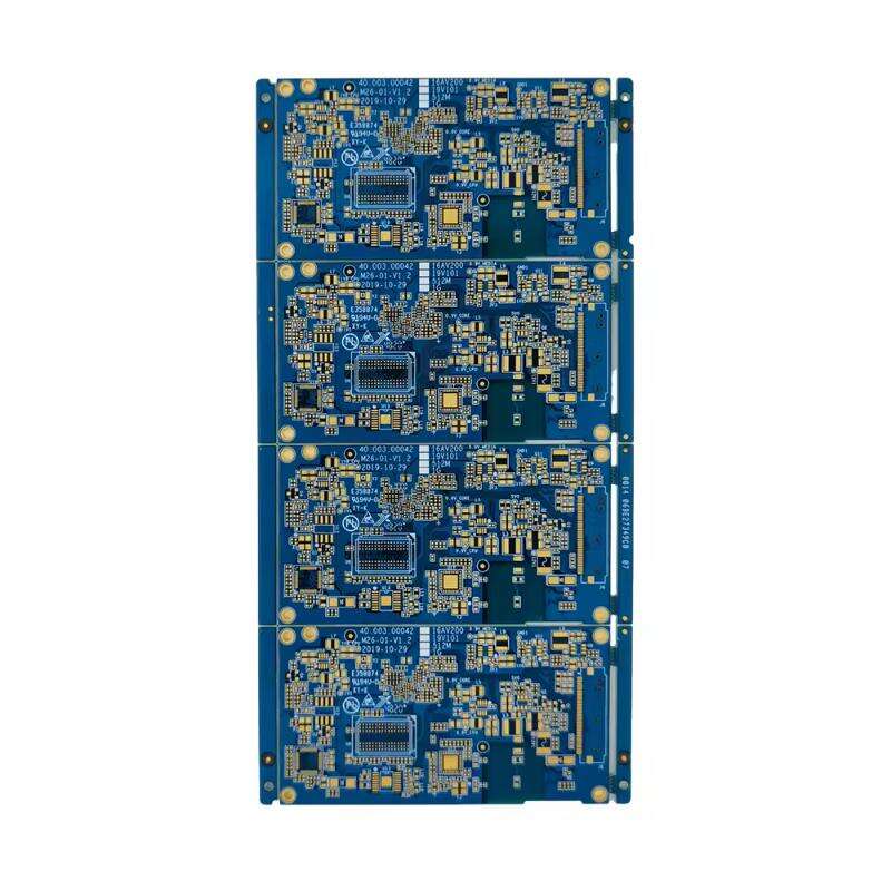
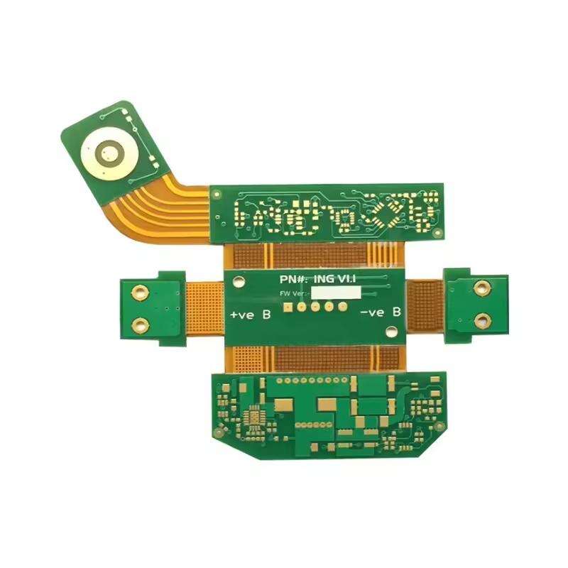
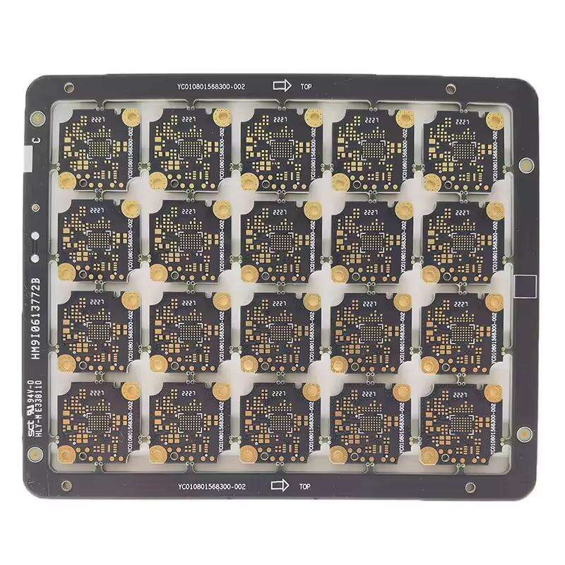
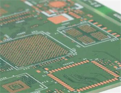
Multilayer PCB (Printed Circuit Board) is an advanced type of circuit board that consists of multiple layers of conductive pathways and insulating material. Unlike single-sided or double-sided PCBs, which have only one or two layers, multilayer PCBs can have three or more layers stacked together. The following table shows the difference between multi-layer circuit boards and single-sided and double-sided circuit boards.
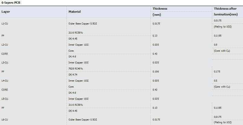
Specifications:
| 4-layers PCB | |||
| Layer | Material | Thickness (mm) | Thickness after lamination(mm) |
| L1-CU | Outer Base Copper 0.5OZ |
0.0175 0.196 0.035 1.03 0.035 0.196 0.0175 |
0.0175 |
| PP | 7628 RC46% | (Plating to 1OZ) | |
| DK:4.74 | 0.1855 | ||
| L2-CU | Inner Copper 1OZ | 1.1 | |
| CORE | Core | (Core with Cu) | |
| DK:4.6 | |||
| L3-CU | Inner Copper 1OZ | ||
| PP | 7628 RC46% | 0.1855 | |
| DK:4.74 | 0.0175 | ||
| L4-CU | Outer Base Copper 0.5OZ | (Plating to 1OZ) | |
Competitive Advantage:
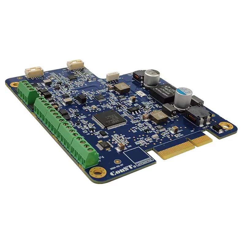
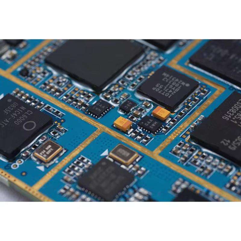
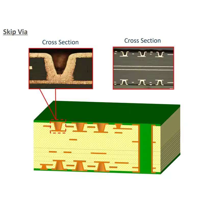
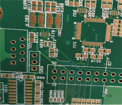
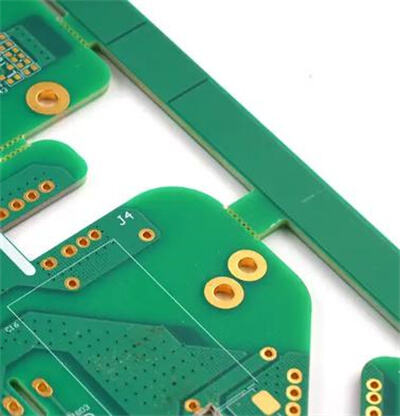
Multilayer printed circuit boards consist of multiple layers of conductive material separated by insulating layers. This structure allows for complex circuits and high component density. The outer layers are defined as the top and bottom layers, which are usually covered with protective materials and provide connection points for electronic components. The inner layers are defined as signal layers, power ground layers, and plane layers. Below is a breakdown of the basic structure of a multilayer PCB.
 EN
EN
 FR
FR
 ES
ES
 PT
PT
 AR
AR
 RU
RU
 KO
KO
 JA
JA
 DE
DE
 NL
NL
 VI
VI
 BG
BG
 HR
HR
 CS
CS
 DA
DA
 FI
FI
 EL
EL
 HI
HI
 IT
IT
 NO
NO
 PL
PL
 RO
RO
 SV
SV
 TL
TL
 IW
IW
 ID
ID
 LT
LT
 SR
SR
 SK
SK
 HU
HU
 TH
TH
 TR
TR
 FA
FA
 GA
GA
 CY
CY
 IS
IS
 HY
HY
 LA
LA
 UK
UK