Description:
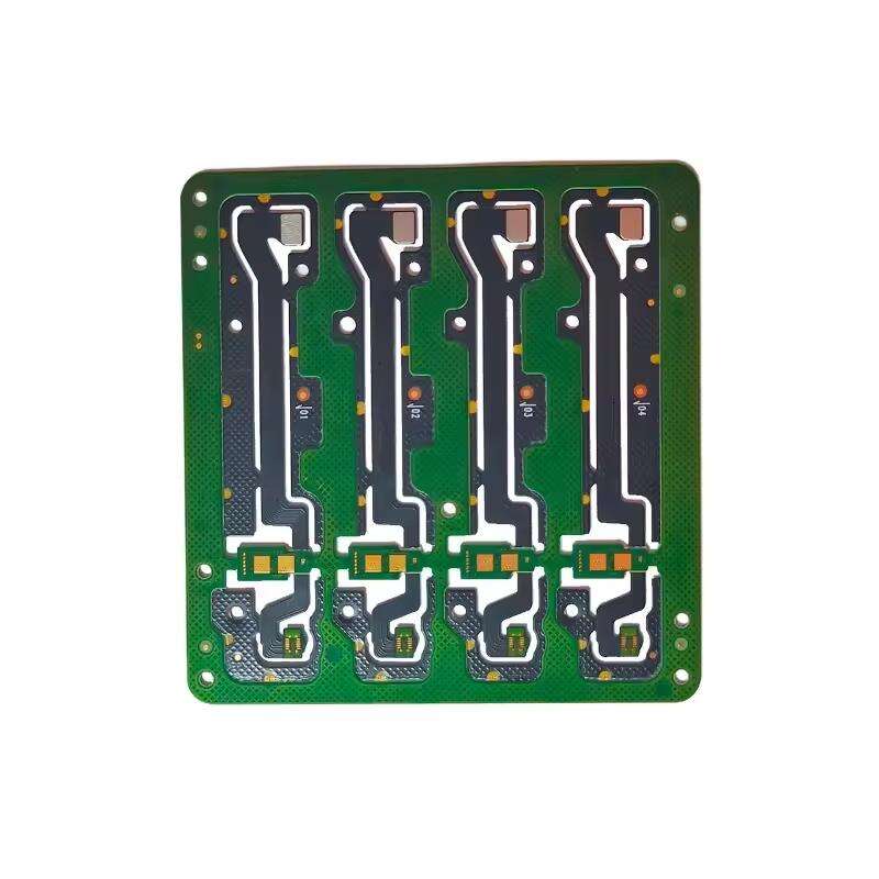
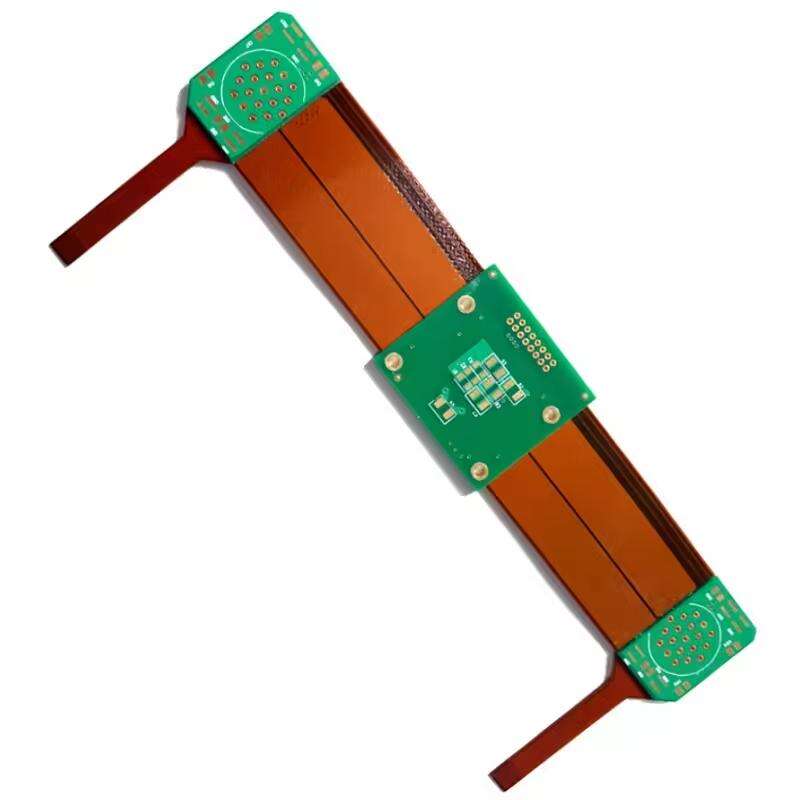
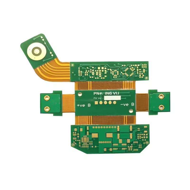
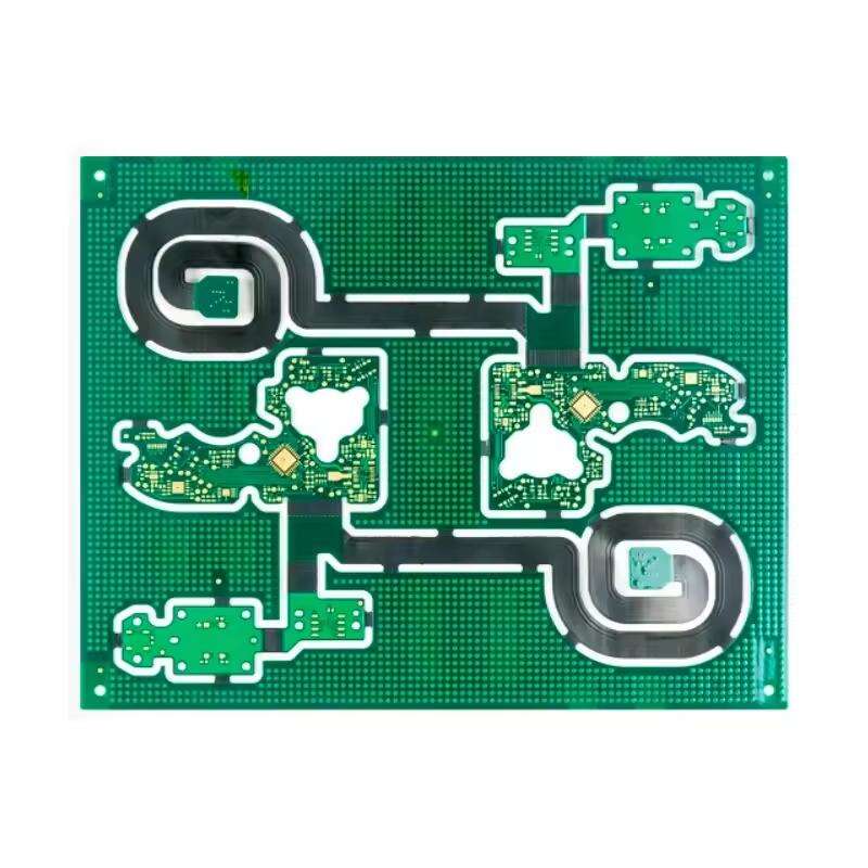
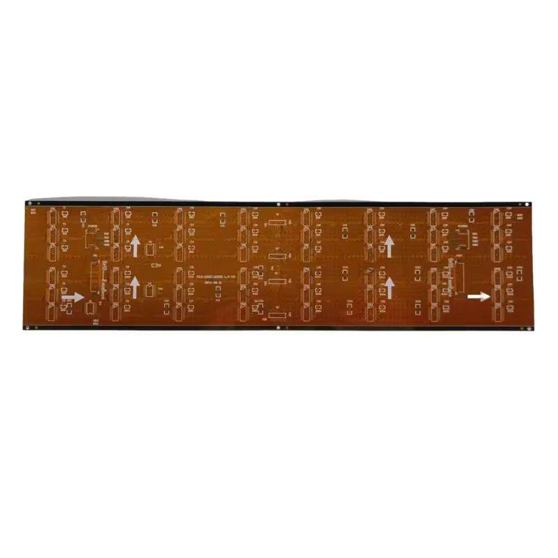
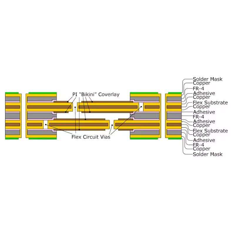
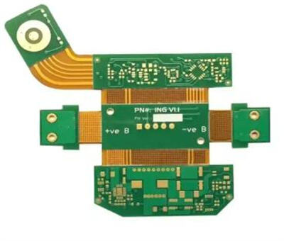
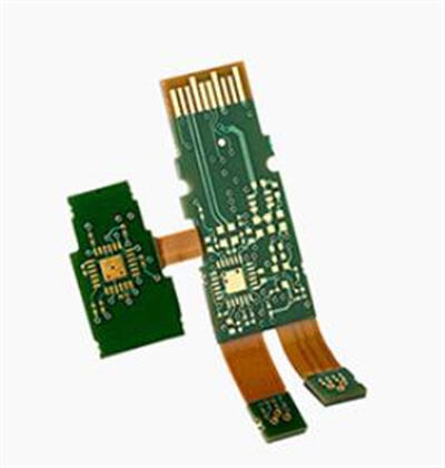
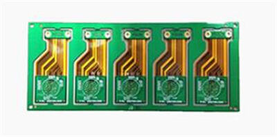
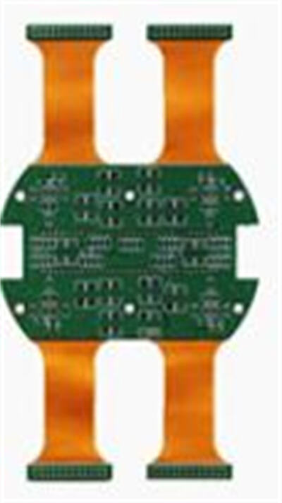
Rigid-flex is especially valuable in applications where space is limited, weight is a constraint, or electronics are subject to mechanical motion. These designs eliminate the need for bulky connectors and cables between rigid boards, improving durability and reducing assembly complexity.
Applications:
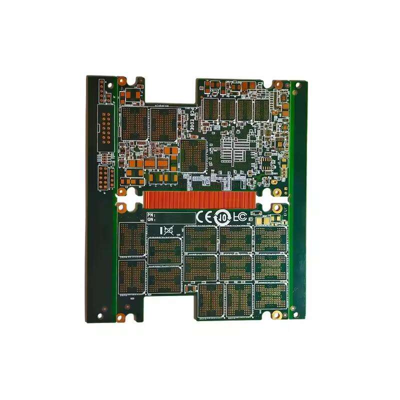
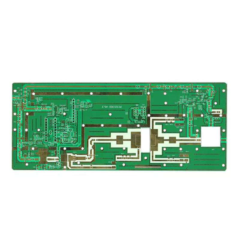
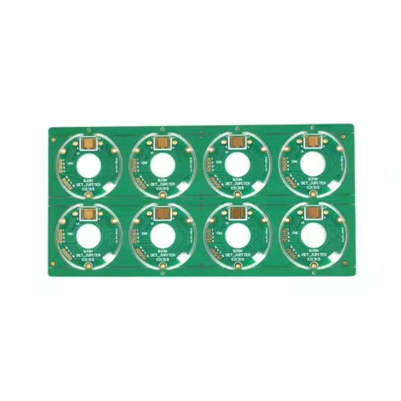
Small size, high reliability, and suitable for complex structural designs; main application areas: consumer and BMS, Automated equipment.
Specifications:
| Feature | Capability | Process Capability | Standard | Speciation |
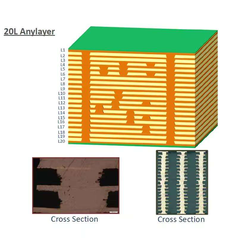
| Layer | 26L | Min.Trace Width/Space | 3mil | 2mil |
| Min. Track/Spacing | 0.065 mm/0.065 mm | Hole size(drilling) | Φ6mil | Φ2mil(laser) |
| Min. Hole/pa Size | 0.10/0.35 mm | Hole size(punching) | Φ20mil | Φ20mil |
| Rigid-Flex Thickness | 0.25-6.0mm | Min. via hole ring | Φ6mil | Φ5mil |
| MAX CU Thickness | 4 OZ | Aspect ratio limits(through holes) | 8:1 | 10:1 (hole size≧D0.30mm) |
| Drilling accuracy | +/-0.05 mm | Aspect ratio limits(blind holes) | 1:1 | 1:1 |
| PTH diameter tolerance | +/-0.05 mm | Layer registration | ±3mils | ±2mils (LDI) |
| MAX WPNL SIZE | 620 mm × 500 mm | |||
| Finish copper (Flex Part) | 0.5-2oz | |||
| Finish copper (Rigid Part) | 1-4oz | |||
| Surface treatment |
ENIG, Electric gold, IM-Ag, Electric Ag, HASL, HASL-LF, IM-Sn, Electric Sn, OSP, Caborn, Pt, NI-Pd-AU |
|||
| Max board thickness: PTH diameter | 13:1 | |||
| Build time | 7-20 days | |||
| RFQ | 1-2 days |
Competitive Advantage:
The versatility of rigid-flex circuit board layouts enables complex and innovative designs that can adapt to non-planar surfaces and accommodate unique geometric shapes, thus pushing the boundaries of electronic device design. The adoption of rigid-flex PCB technology can contribute to more sustainable and environmentally friendly electronic devices by reducing material waste and promoting energy-efficient designs. while rigid circuit areas provide stability and strength for other areas of the product that need increased durability and shock absorption.
 EN
EN
 FR
FR
 ES
ES
 PT
PT
 AR
AR
 RU
RU
 KO
KO
 JA
JA
 DE
DE
 NL
NL
 VI
VI
 BG
BG
 HR
HR
 CS
CS
 DA
DA
 FI
FI
 EL
EL
 HI
HI
 IT
IT
 NO
NO
 PL
PL
 RO
RO
 SV
SV
 TL
TL
 IW
IW
 ID
ID
 LT
LT
 SR
SR
 SK
SK
 HU
HU
 TH
TH
 TR
TR
 FA
FA
 GA
GA
 CY
CY
 IS
IS
 HY
HY
 LA
LA
 UK
UK