
 EN
 FR
 ES
 PT
 AR
 RU
 KO
 JA
 DE
 NL
 VI
 BG
 HR
 CS
 DA
 FI
 EL
 HI
 IT
 NO
 PL
 RO
 SV
 TL
 IW
 ID
 LT
 SR
 SK
 HU
 TH
 TR
 FA
 GA
 CY
 IS
 HY
 LA
 UK
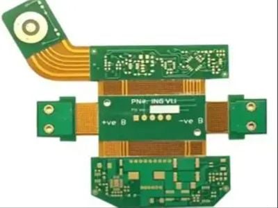
High-density interconnect (HDI) PCB design is crucial for modern electronic applications, particularly where space & performance are paramount. This article will address key buyer concerns regarding, blind, and buried vias in pcb connection , providing insights into specifications, installation challenges, and supplier sourcing. By understanding these aspects, purchasing managers and engineers can make informed decisions that align with their project requirements. 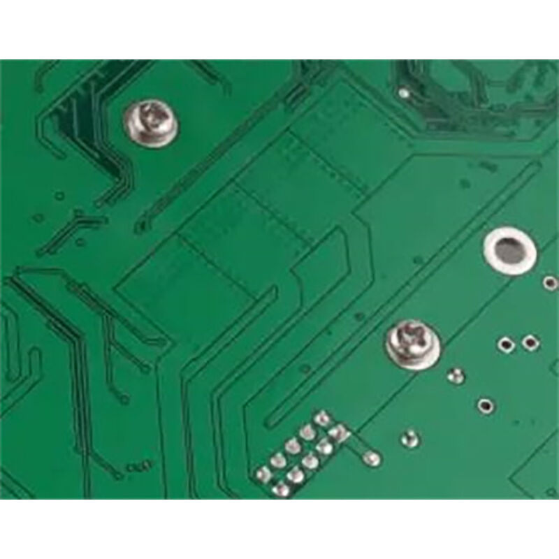
Understanding High-Density Interconnect (HDI) PCB Design Specifications
HDI PCBs utilize advanced manufacturing techniques to achieve higher wiring density per unit area compared to traditional PCBs. This is primarily accomplished through the use of microvias—small vias that can be as fine as 75 micrometers in diameter—along with blind and buried vias.
Microvias are typically created using laser drilling, which allows for precise targeting of specific layers without damaging adjacent layers. They are essential in reducing the overall footprint of the PCB, making them ideal for compact devices like smartphones and wearable technology.
Blind vias connect an outer layer to one or more inner layers but do not go through the entire board. In contrast, buried vias connect only inner layers, providing additional routing options without increasing board thickness. The choice between these via types depends on factors such as design complexity, layer count, and final application requirements.
Key specifications to consider include the via diameter, aspect ratio (the ratio of the via's depth to its diameter), and the copper plating specifications. These choices directly impact performance, including signal integrity and thermal management, making it essential for buyers to specify their requirements clearly when requesting quotes.
How to Choose the Right Microvia and Blind/Buried Vias for Your Project
Selecting the appropriate microvia and blind/buried vias starts with understanding your project’s specific needs. For high-frequency applications, microvias are often preferable due to their lower inductance and capacitance, which contribute to enhanced signal integrity.
When choosing between blind and buried vias, consider the following:
Layer Configuration: If your design requires multiple layer interconnections & routing, buried vias may be more advantageous as they do not impact the outer layers, maintaining a clean design.
Thermal Performance: For applications where heat management is critical, ensure the selected vias allow for efficient heat dissipation. Microvias can help with thermal management in densely packed circuits.
Manufacturing Capabilities: Ensure your selected supplier has the capability to manufacture the desired via types. Not all manufacturers can handle microvias or buried vias effectively due to the technical challenges involved.
Cost Implications: While microvias and buried vias can enhance performance, they may also increase production costs. Discuss with your supplier to understand the trade-offs involved and how they can align with your budget.
Common Installation Challenges with HDI PCBs and Their Solutions
Installing HDI PCBs presents unique challenges, particularly due to their complex structures. Some common challenges include:
Alignment Issues: Precise alignment is critical during assembly, especially with small components and intricate via patterns. Using advanced pick-and-place machines with vision systems can mitigate these issues.
Thermal Stress: The high density of connections can cause localized heating during soldering. Implementing controlled thermal profiles during manufacturing can minimize thermal stress, ensuring reliability.
Solderability: Microvias may be challenging to solder due to their size and geometry. Utilizing appropriate solder pastes and techniques, such as selective soldering, can improve solder joint integrity.
Quality Control: Due to the complexity of HDI boards, inspection becomes crucial. Employ automated optical inspection (AOI) and X-ray inspection for hidden vias to ensure manufacturing quality before deployment.
Addressing these challenges proactively helps ensure that your HDI PCB performs reliably throughout its intended lifecycle.
Where to Source Reliable Suppliers for HDI PCB Components
Sourcing reliable suppliers for HDI PCB components requires careful evaluation to ensure they meet quality and capability standards. Consider the following steps:
Industry Reputation: Research potential suppliers’ reputations within the industry. Look for manufacturers with a proven track record in HDI PCB production and positive customer feedback.
Certifications: Check for industry certifications such as ISO 9001 or IPC standards, which indicate a commitment to quality management and technical expertise.
Manufacturing Capabilities: Ensure that the supplier has the necessary equipment and technology for HDI production, including laser drilling for microvias and automated assembly processes.
Communication and Support: Choose a supplier that offers robust customer support and clear communication channels. This will help in addressing any concerns during the design and manufacturing phases.
Sample Testing: Before committing to a large order, request samples to evaluate the quality of the PCBs. This can help identify any potential issues before full-scale production.
What Buyers Need to Know
When preparing to purchase HDI PCBs, buyers should keep several critical factors in mind:
Specification Clarity: Clearly outline your project requirements, including dimensions, layer counts, via types, and any specific performance criteria. This helps suppliers provide accurate quotes and timelines.
Lead Times: Discuss lead times with suppliers, especially if your project has tight deadlines. Understand how design complexity and order volume can impact production schedules.
Quality Checks: Implement a robust quality inspection process. Ensure that suppliers conduct thorough inspections during production and provide documentation for traceability.
Customization Options: If your project requires unique design features or materials, confirm the supplier’s customization capabilities. Discuss potential costs and timelines associated with custom requests.
By understanding these factors, purchasers can foster a successful partnership with manufacturers and ensure the delivery of high-quality HDI PCBs that meet their specific needs.
In summary, navigating the complexities of pcb board design online and manufacturing requires a well-informed approach. By focusing on specifications, sourcing reliable suppliers, and anticipating challenges, buyers can make strategic decisions that enhance their projects' success.