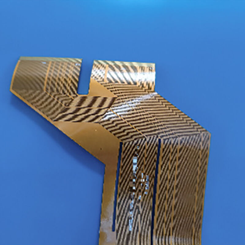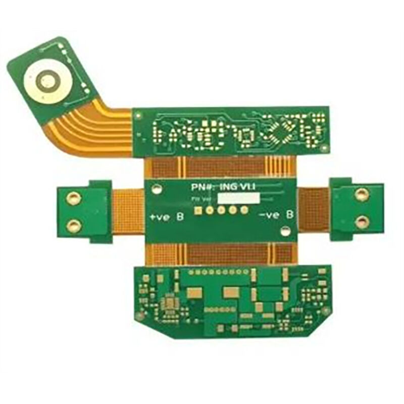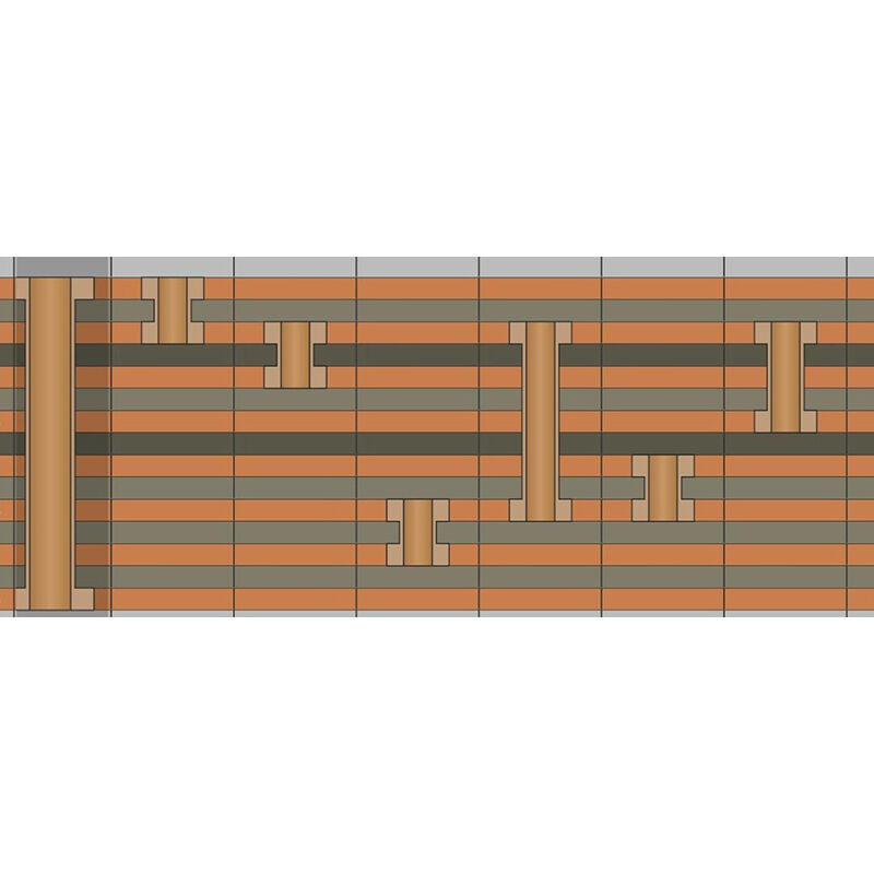
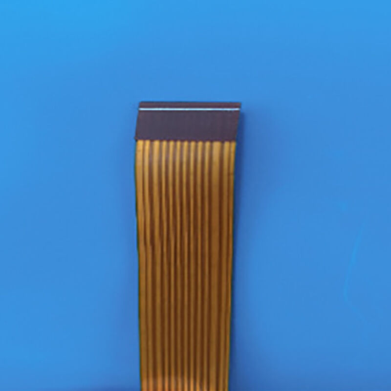
Flex PCBs are built on flexible polyimide or polyester films, allowing them to conform to complex shapes or dynamic mechanical requirements. Rigid flex PCBs combine multiple rigid layers with flexible layers, laminated together into a single structure. This hybrid approach reduces interconnects, enhances signal reliability, and simplifies enclosure design.
Flex PCBs are thin and lightweight, allowing for compact designs that save space and reduce the overall weight of electronic devices, which is particularly important for aerospace, automotive, and wearable applications.
| Feature | Capability | Feature | Capability |
| Layer | 1-12 | Min. bend radius of single layer | 3‐6 times of board thickness |
| Board thickness (without stiffener) | 4‐40 mil | Min. bend radius of double layer | 7‐10 times of board thickness |
| Tolerance of single layer | ±1.0mil | Min. bend radius of multi‐layer | 10‐15 times of board thickness |
| Tolerance of double layer (≤12mil) | ±1.2 mil | Min. mechanical drill hole | 4 mil |
| Tolerance of multi‐layer (≤12mil) | ±1.2 mil | Inner Layer Trace/ Space | 2/ 2 mil |
| Tolerance of multi‐layer (12mil‐32mil) | ±8% | Outer Layer Trace/ Space | 2/ 2 mil |
| Tolerance of board thickness (including PI stiffener) | ±10% | Solder mask color | Green\Black |
| Min. board size | 0.0788" *0.1576" (without bridge) 0.3152" * 0.3152" (with bridge) | Surface treatment | HASL, ENIG, ENEPIG, Electrolytic Nickel Gold, Soft gold, Hard gold, Immersion silver and OSP, Immersion tin |
| Max. board size | 8.668" * 27.5" | Laser accuracy (Routing) | ±2 mil |
| Impedance control tolerance | ±4Ω (≤50Ω), ±7% (>50Ω) | Punching accuracy (Routing) | ±2 mil ‐ ±6 mil |
| Min. overlay bridge | 8 mil |
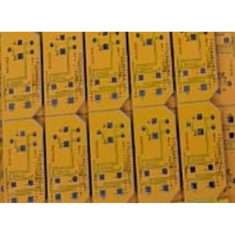
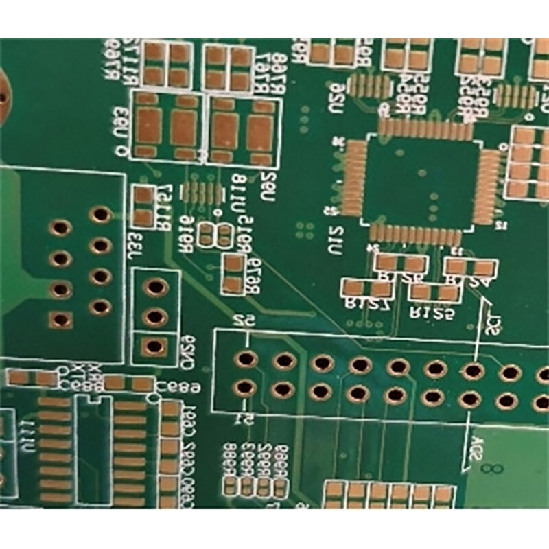
Flex PCBs are widely used across various industries due to their unique combination of flexibility, durability, and design versatility.
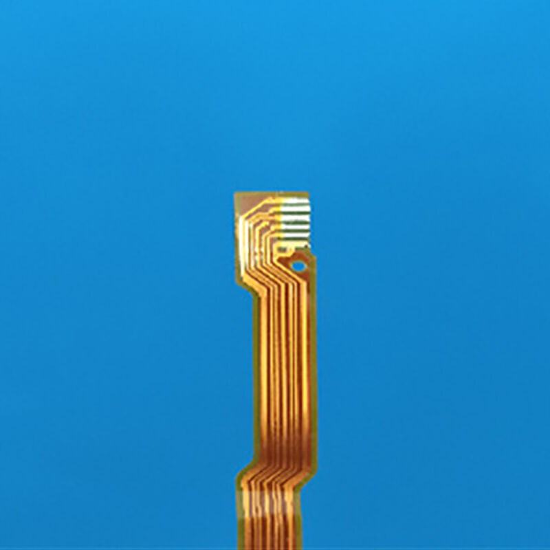
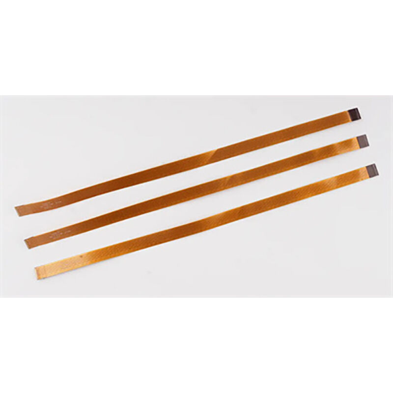
The flexible nature of these materials allows flex PCBs to bend, fold, and twist without causing damage to the circuits or impacting their functionality.
 EN
EN
 FR
FR
 ES
ES
 PT
PT
 AR
AR
 RU
RU
 KO
KO
 JA
JA
 DE
DE
 NL
NL
 VI
VI
 BG
BG
 HR
HR
 CS
CS
 DA
DA
 FI
FI
 EL
EL
 HI
HI
 IT
IT
 NO
NO
 PL
PL
 RO
RO
 SV
SV
 TL
TL
 IW
IW
 ID
ID
 LT
LT
 SR
SR
 SK
SK
 HU
HU
 TH
TH
 TR
TR
 FA
FA
 GA
GA
 CY
CY
 IS
IS
 HY
HY
 LA
LA
 UK
UK