Početna Stranica > Proizvodi > Izrada Pločica Za Tiskane Ploče > Čvrsta - fleksibilna PCB
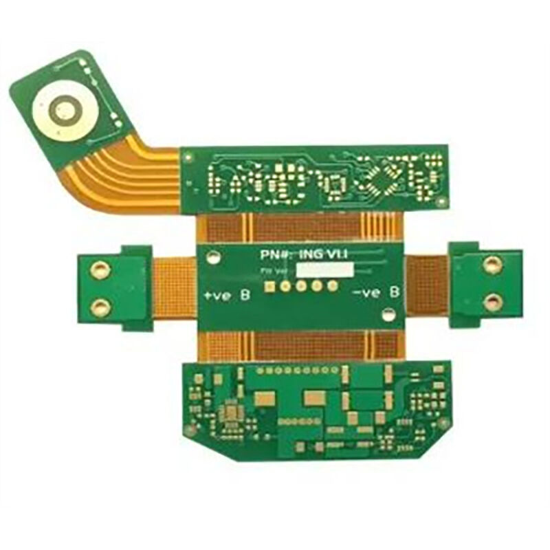
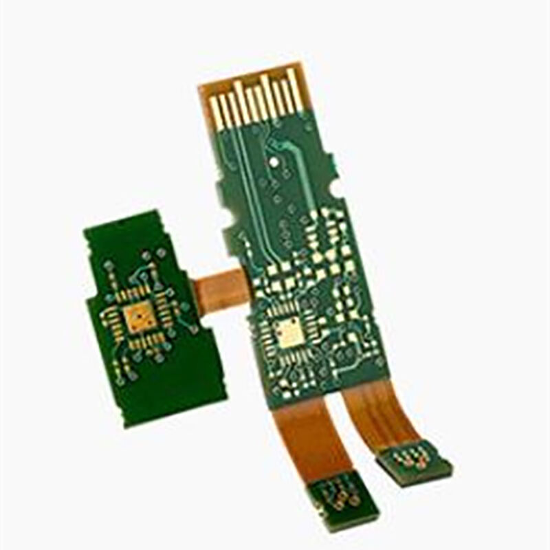
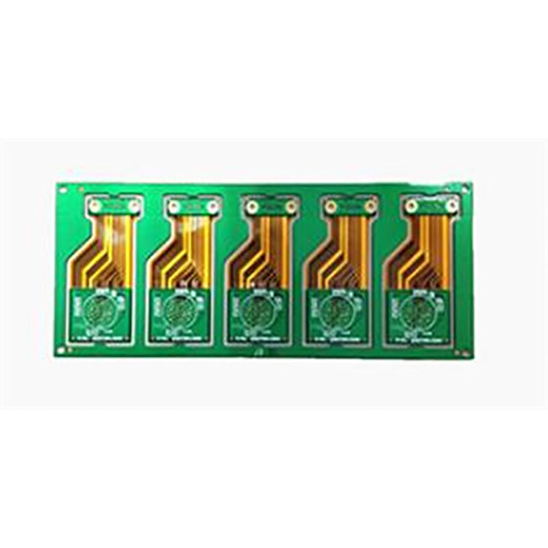
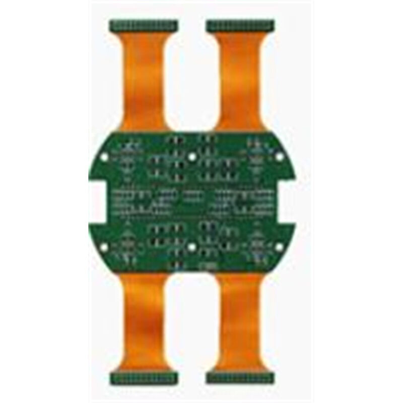
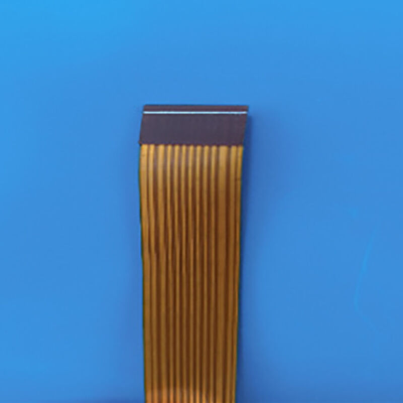
Stroga fleksibilnost posebno je vrijedna u primjenama gdje je prostor ograničen, težina je ograničenje ili elektronika podložna mehaničkom pokretu. Ti dizajni eliminišu potrebu za gomilanim spojevima i kablovima između čvrstih ploča, poboljšavajući izdržljivost i smanjujući složenost montaže.
U skladu s člankom 3. stavkom 1. stavkom 2. ovog Pravilnika, za potrebe primjene ovog Pravilnika, proizvođač mora imati pravo na:
| Značajka | Moćnost | Mogućnost obrade | Standard | Specijacija |
| Složak | 26L | Min.Širina tragova/prostor | 3MIL | 2MIL |
| - Min. - Što? Sljedeći članak | s druge strane, za sve proizvode koji sadrže: | Veličina rupe (bušenje) | φ6mil | p2mil (laser) |
| - Min. - Što? Veličina rupe/pa | smanjenje dužine | Veličina rupe (perforacija) | φ20 mil | φ20 mil |
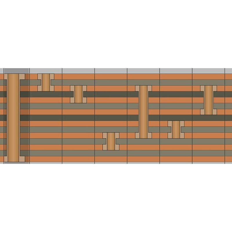
| Čvrsta i fleksibilna debljina | smanjenje | Min. kroz prsten s rupom | φ6mil | φ5m |
| Max CU debljina | 4 oz | U slučaju da je to potrebno, potrebno je utvrditi granicu razmjera aspekta. | 8:1 | (Ustanovljeni broj) |
| Preciznost bušenja | smanjenje | U slučaju da je to potrebno, potrebno je utvrditi: | 1:1 | 1:1 |
| U slučaju da je to potrebno, potrebno je utvrditi: | smanjenje | Registracija sloja | ± 3 milje | svaka vrsta vozila |
| U skladu s člankom 4. stavkom 2. | 620 mm × 500 mm | |||
| S druge strane, u slučaju da se ne primjenjuje, ne smije se upotrebljavati. | 0,5-2 oz | |||
| S druge strane, u slučaju da se ne upotrebljava, ne smije se upotrebljavati. | 1-4 oz | |||
| Obrada površine | U skladu s člankom 3. stavkom 1. | |||
| U slučaju da je to potrebno, za svaki proizvod, potrebno je upotrebiti sljedeće elemente: | 13:1 | |||
| Vrijeme izrade | 7-20 dana | |||
| Upit za ponudu | 1-2 dana |
Sveobuhvatnost postavki rigidno-flexnih ploča omogućuje složene i inovativne dizajne koji se mogu prilagoditi ne-planoj površini i prilagoditi jedinstvenim geometrijskim oblicima, čime se pomakaju granice dizajna elektroničkih uređaja. Uvođenje tehnologije čvrstih i fleksibilnih PCB-a može doprinijeti održivijem i ekološki prihvatljivim elektroničkim uređajima smanjenjem otpada materijala i promicanjem energetski učinkovitih dizajna. Dok čvrsta područja kola pružaju stabilnost i snagu drugim područjima proizvoda koja trebaju povećanu trajnost i
 EN
EN
 FR
FR
 ES
ES
 PT
PT
 AR
AR
 RU
RU
 KO
KO
 JA
JA
 DE
DE
 NL
NL
 VI
VI
 BG
BG
 HR
HR
 CS
CS
 DA
DA
 FI
FI
 EL
EL
 HI
HI
 IT
IT
 NO
NO
 PL
PL
 RO
RO
 SV
SV
 TL
TL
 IW
IW
 ID
ID
 LT
LT
 SR
SR
 SK
SK
 HU
HU
 TH
TH
 TR
TR
 FA
FA
 GA
GA
 CY
CY
 IS
IS
 HY
HY
 LA
LA
 UK
UK