Почетна страница > Производи > Izrada Ploča Štampanih Kola > Врховна површина високе густине (HDI)
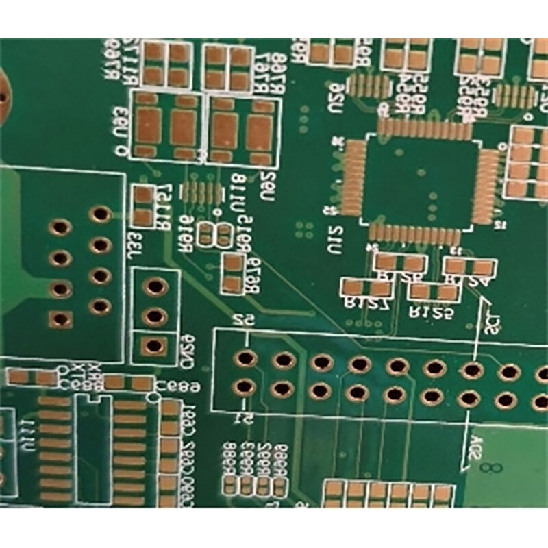
ПКБ-и са интерконектом високе густине (ХДИ) даље се развијају на овој основи, користећи микровије, рутирање фине линије, слепе и закопане вије и дизајне вије-ин-пад-а како би се постигло чвршће постављање компоненти и перформансе
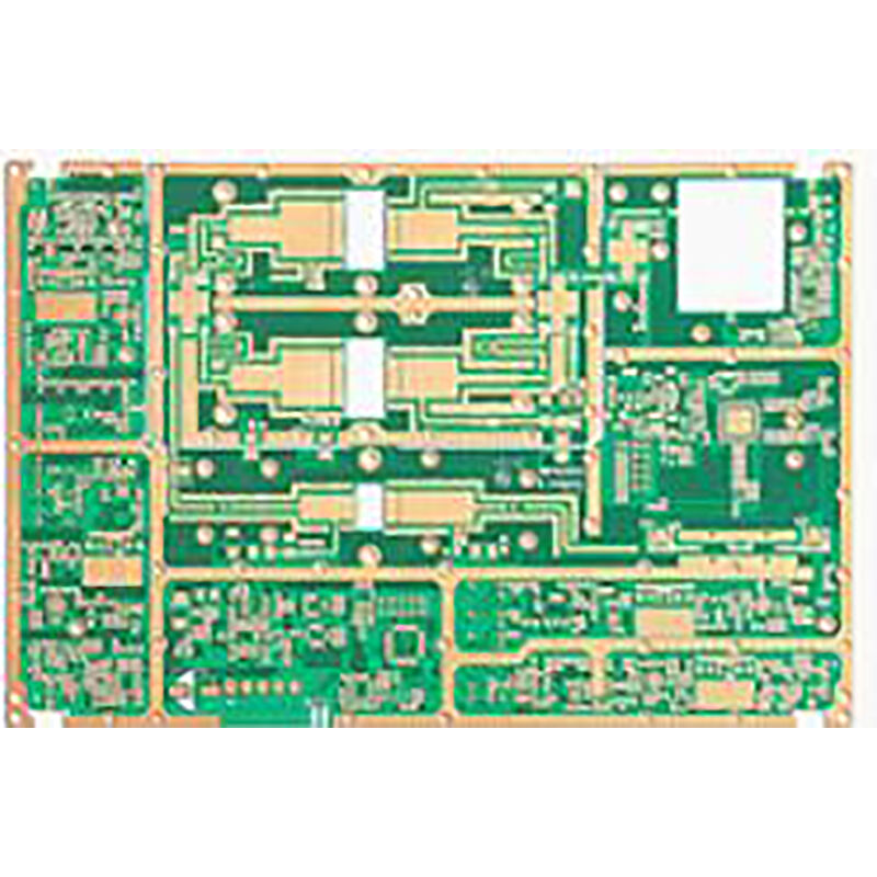
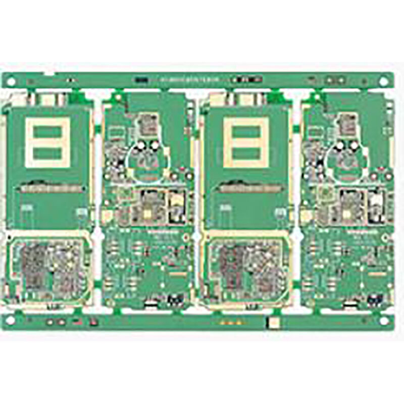
HDI PCB (High Density Interconnect PCB) се углавном користи у компактним, високоперформансним електронским производима. Типична подручја примене укључују:
Конзимер, рачунар и мреже, аутомобил, медицинска.
| Особност | Способност | Особност | Способност |
| Tipovi provodnika | Slepi provodnik, zakopani provodnik, provodnik kroz rupu | Min. mehaničko bušenje | 0,15 мм |
| Број слојева | Do 60 slojeva (potrebna procena iznad 30 slojeva) | Min. lasersko bušenje | Стандардни 4 мили, 3 мили захтевају процену (одговарају јединственој 106ПП). |
| HDI konstrukcije | 1+Н+1, 2+Н+2,..., 6+Н+6 ((≥6 наређења захтевају процену) | Maks. lasersko bušenje | 8 ml (одговарајућа диелектрична дебљина не може бити већа од 0,15 mm) |
| Медни тегови (свршени) | 18μm-70μm | Min. bušenje sa kontrolisanom dubinom | PTH: 0,15 mm; NPTH: 0,25 mm |
| Minimalna trasa/razmak | 0,065mm/0,065mm | Однос аспекта | Максимално 14:1; процени ако је веће. |
| Debljina PCB | 0,1-8,0mm (potrebna procena za manje od 0,2mm ili veće od 6,5mm) | Minimalni most za otpornik protiv lemljenja | 4мл ((зелена, ≤1ОЗ) |
| Макс. -Макс. Димензија ПЦБ-а (завршена) | 2-20 слојева, 21*33 инча; дужина ≤ 1000 мм; проценити ако је кратка страна > 21 инч | 5мл ((друге боје, ≤1ОЗ) | |
| Opseg prečnika provrta sa punjenjem smolom | 0,254–6,5 mm |
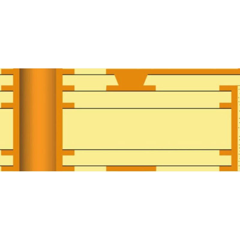
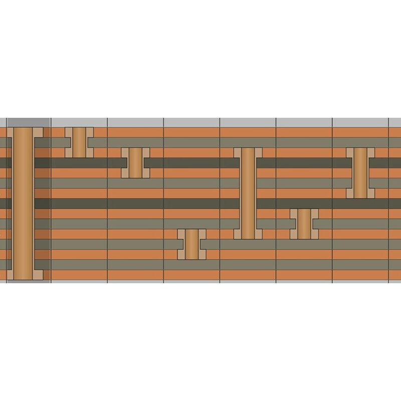
Структуре за складиштење ХДИ ПЦБ пружају дизајнерима већу флексибилност у распореду слојева, постављању компоненти и опцијама рутинга, омогућавајући ефикасну употребу доступног простора и оптимизацију распореда ПЦБ-а. Уобичајене структуре за спајање ХДИ ПЦБ приказане су на сљевачком дијаграму.
 EN
EN
 FR
FR
 ES
ES
 PT
PT
 AR
AR
 RU
RU
 KO
KO
 JA
JA
 DE
DE
 NL
NL
 VI
VI
 BG
BG
 HR
HR
 CS
CS
 DA
DA
 FI
FI
 EL
EL
 HI
HI
 IT
IT
 NO
NO
 PL
PL
 RO
RO
 SV
SV
 TL
TL
 IW
IW
 ID
ID
 LT
LT
 SR
SR
 SK
SK
 HU
HU
 TH
TH
 TR
TR
 FA
FA
 GA
GA
 CY
CY
 IS
IS
 HY
HY
 LA
LA
 UK
UK